AMD threatens to go medieval on Nvidia with Epyc and Instinct: What we know so far
AMD teased its next-generation of AI accelerators at CES 2026, with CEO Lisa Su boasting the the MI500-series will deliver a 1,000x uplift in performance over its two-year-old MI300X GPUs.
That sounds impressive, but, as usual, the devil is in the details. In a press release that followed Monday's keynote, AMD clarified those estimates are based on a comparison between an eight-GPU MI300X node and an MI500 rack system with an unspecified number of GPUs. That's not exactly an apples-to-apples comparison.
According to AMD its next-gen MI500X-series GPUs will deliver an 1000x performance boost over the now two-year-old MI300X. What that actually means? Hard to say - Click to enlarge
The math works out to eight MI300Xs that are 1000x less powerful than X-number of MI500Xs. And since we know essentially nothing about the chip besides that it'll ship in 2027, pair TSMC's 2nm process tech with AMD's CDNA 6 compute architecture, and use HBM4e memory, we can't even begin to estimate what that 1000x claim actually means.
Calculating AI performance isn't as simple as counting up the FLOPS. It's heavily influenced by network latency, interconnect and memory bandwidth, and the software used to distribute the workloads across clusters. These factors affect LLM inference performance differently than training or video generation. Therefore, greater than 1000x therefore could mean anything AMD wants it to.
Having said that, if AMD wants to stay competitive with Nvidia, the MI500-series will need to deliver performance on par with if not better than Nvidia's Rubin Ultra Kyber racks. According to Nvidia, when the 600kW systems make their debut next year, they'll deliver 15 exaFLOPS of FP4 compute, 5 exaFLOPS of FP8 for training, 144 TB of HBM4e, and 4.6 PB/s of memory bandwidth.
Breaking down the Instinct MI400-series
Details on the MI500 may be razor thin, but we're starting to get a better picture of what AMD's MI400 series GPUs and rack systems will look like.
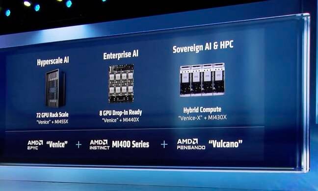
AMD's MI400 series GPUs will span three configurations from hyperscale and enterprise AI to mixed AI and HPC - Click to enlarge
At CES, AMD revealed MI400 would be offered in at least three flavors:
- MI455X — an AI-optimized GPU that'll power its Helios rack systems starting later this year.
- MI440X — a presumably lower-end version of the MI455 that'll be offered in a more conventional eight-way GPU box, like those used by the MI355x and MI325.
- MI430X — a mixed-use GPU designed to balance the demands of both high-performance computing and AI, and will be deployed in at least two upcoming supercomputers.
AMD joins the rack-scale race with Helios
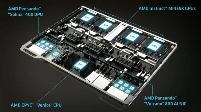
AMD CEO strutted out a Helios compute blade complet with 4x MI455X GPUs and a Venice CPU at CES on Monday - Click to enlarge
For the AI crowd, AMD's MI455X-powered Helios racks are the ones to watch, as OpenAI, xAI, and Meta are expected to deploy them at scale.
Each of these accelerators promise around 40 petaFLOPS of dense FP4 inference performance or 20 petaFLOPS of FP8 for training, and 432 GB of HBM4 good for 19.6 TB/s and 3.6 TB/s of interconnect bandwidth for chip-to-chip communications.
Presumably, these chips will support higher precision datatypes commonly used in training and image models, but AMD has yet to spill the beans on those figures.
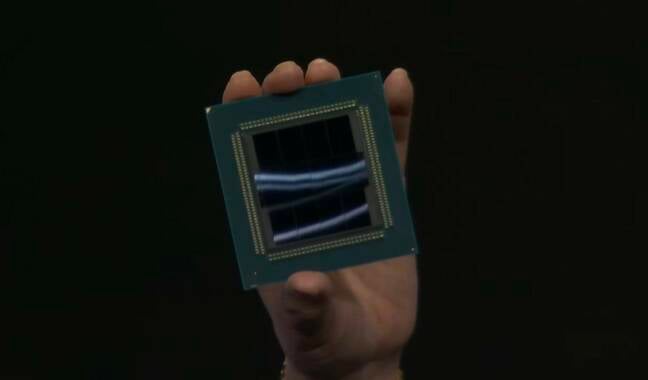
At the very least, we now know what the chip will look like. On stage, Su revealed the MI455X package, which will use 12 3D-stacked I/O and compute dies fabbed on TSMC's 2 nm and 3 nm process nodes. All will be fed by what to our eyes appears to be 12 36 GB HBM4 stacks.
There it is. MI455X in the silicon. - Click to enlarge
Helios will employ 72 of these chips with one Epyc Venice CPU for every four GPUs forming a node.
Venice in the silicon
Speaking of Venice, at CES we also got our best look yet at AMD's highest-core-count Epyc ever.
The image isn't the sharpest, but we can just make out what appear to be eight 32-core CCDs and a pair of I/O dies on the Venice CPU package - Click to enlarge
The chips will be available with up to 256 Zen 6 cores and will feature twice the memory and GPU bandwidth compared to last gen. By GPU bandwidth, we assume AMD is talking about PCIe lanes, which tells us that we're looking at 128 lanes of PCIe 6.0 connectivity. To double the memory bandwidth over Turin, meanwhile, we estimate AMD will need 16 channels of DDR5 8800.
To fit that many cores into a single chip, Venice appears to use a new packaging technique with what looks like eight 32-core chiplets and two I/O dies. There also appear to be eight tiny chiplets on either side of the I/O chipsets, though it isn't immediately obvious what purpose they serve.
We don't know yet whether the version of Venice Su was holding in her keynote is using one of AMD's compact or frequency-optimized cores. Since at least 2023, AMD has offered two versions of its Zen cores: a larger, higher-clocking version and a smaller, more compact version that doesn't clock as high.
While that might sound an awful lot like Intel's E-cores, both AMD's Zen and Zen C cores use the same microarchitecture. Intel's E-cores use a different architecture and cache layout from its P-cores. As a result, they often lack advanced functionality like AVX-512 and matrix accelerators.
The only differences between AMD's cores is one can be packed more densely with 16 cores per core complex die (CCD) versus eight, operating at lower frequencies with slightly less cache per core.
If AMD can address the latter point, there may not be a need to differentiate between the two in the Zen 6 generation. We'll just have high-core count SKUs that don't clock as high as the lower-core-count versions like they always have.
Alongside the "standard" Venice SKUs, AMD is once again offering an "X" variant of the part for high performance computing. AMD's X chips have historically featured 3D-stacked cache dies located under or on top of the CCD, boosting the L3 cache significantly. Genoa-X, AMD's last datacenter X chip could be kitted out with more than a terabyte of L3 in its highest-end configuration.
Faster networking
We don't have a lot more information on AMD's next-gen networking stack, but we know that alongside the new CPUs and GPUs, Helios will also feature two new NICs from its Pensando division for rack-to-rack communications across the cluster.
Alongside the 12 Vulcano NICs, the Helios compute blade will also use Pensando's Silina 400 DPU - Click to enlarge
This includes up to twelve 800 Gbps Volcano NICs (three per GPU) which form the scale-out compute fabric — what we call the backend network that allows workloads to be distributed across multiple nodes or in this case racks.
The systems will also feature Pensando's Solina data processing unit, which is designed to offload things like software-defined networking, storage, and security so the CPUs and GPUs can focus on generating tokens or training models.
To stitch Helios's 72 GPUs into one great big accelerator, AMD is using Ultra Accelerator Link (UALink) — an open alternative to Nvidia's NVLink — tunneled over Ethernet.
At least for HPE's implementation of the rack, Broadcom's Tomahawk 6 will handle switching.
There are only so many ways to connect the chips, but at 102.4 Tbps, we estimate AMD will need 12 Tomahawk 6 ASICs spread across six switch blades. Earlier renderings of Helios appeared to show five switch blades which threw us for a bit of a loop, but we've since learned the actual racks will feature six.
Giving Nvidia a run for its money
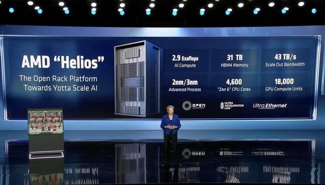
Combined, the Helios rack's 72 GPUs promise to deliver 2.9 exaFLOPS of dense FP4 performance, 1.4 exaFLOPS at FP8, 31 TB of HBM4, and 1.4 PB/s of memory bandwidth. That puts it in the same ballpark and in some cases faster than Nvidia's newly unveiled Vera Rubin NVL72 rack systems, which we looked at earlier this week.
And if you're not ready to drop a few million bucks on a rack-scale system, AMD will also offer the MI440X in an eight-way configuration that, from what we've gathered, will use the same OAM form factor as the MI355X and MI325X. These systems will compete with Nvidia's Rubin NVL8 boxes which pair eight GPUs with an x86-based compute platform for space in the enterprise.
For all the fervor around rackscale, AMD expects this form factor to remain quite popular with enterprise customers that can't, for one reason or another, run their models in the cloud or access them via a remote API.
- Luggable datacenter: startup straps handles to server with 4 H200 GPUs
- AMD clocks in with higher CPU speeds, leaves architecture untouched
- Every conference is an AI conference as Nvidia unpacks its Vera Rubin CPUs and GPUs at CES
- Tired of sky-high memory prices? Buckle up, we're in this for the long haul
While we don't have all the details just yet, it looks like AMD won't just be competing with Nvidia on AI performance, but on HPC perf as well.
The MI430X will feature the same load out of HBM4 as the MI455X at 432 GB and 19.6 TB/s. But where MI455X is all about AI, the MI430X will use a different set of chiplets, giving it the flexibility to run at either FP64 or FP32 for HPC, FP8 or FP4 for AI, or a combination of the two as is quickly becoming the fashion.
Much like with the MI440X, AMD hasn't disclosed the floating point perf of the MI430X, but using publicly available information, the wafer wizards at Chips and Cheese suggest it could be north of 200 teraFLOPS.
Whatever the chip's actual floating point performance actually ends up being, we know it'll be achieved in hardware. This sets AMD apart from Nvidia, which is relying on emulation to boost FP64 performance of its Rubin GPUs to 200 teraFLOPS.
We expect AMD will have more to share on its Venice CPUs and the rest of its MI400-series accelerators closer to launch, which is expected sometime in the second half of 2026. ®


