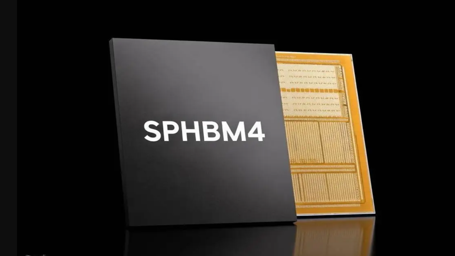
New 'serial' tech will significantly reduce the cost of memory — HBM memory, that is, the sort of RAM only AI hyperscalers can use, but hey, at least they won't go after consumer RAM, or would they?
SPHBM4 uses serialization and organic substrates to lower HBM packaging costs while keeping bandwidth memory exclusive to hyperscale AI systems.

(Image credit: Sohu)
- SPHBM4 cuts pin counts dramatically while preserving hyperscale-class bandwidth performance
- Organic substrates reduce packaging costs and relax routing constraints in HBM designs
- Serialization shifts complexity into signaling and base logic silicon layers
High bandwidth memory has evolved around extremely wide parallel interfaces, and that design choice has defined both performance and cost constraints.
HBM3 uses 1024 pins, a figure that already pushes the limits of dense silicon interposers and advanced packaging.
The JEDEC Solid State Technology Association is developing an alternative known as Standard Package High Bandwidth Memory 4 (SPHBM4), which reduces the physical interface width while preserving total throughput.
HBM4 interface doubles HBM3
The standard HBM4 specification doubles the HBM3 interface width to 2,048 pins, with digital signals passing through each contact to raise aggregate throughput.
This scaling approach improves bandwidth, but it also increases routing complexity, substrate demands, and manufacturing expense, which concerns system designers.
The planned SPHBM4 device uses 512 pins and relies on 4:1 serialization while operating at a higher signaling frequency.
In bandwidth terms, one SPHBM4 pin is expected to carry the equivalent workload of four HBM4 pins.
Sign up to the TechRadar Pro newsletter to get all the top news, opinion, features and guidance your business needs to succeed!
This approach shifts complexity away from pin count and toward signaling technology and base logic design.
Reducing pin count allows wider spacing between contacts, which directly affects packaging options.
JEDEC states that this relaxed bump pitch enables connection to organic substrates rather than silicon interposers.
Silicon substrates support very high interconnect densities with pitches above 10 micrometers, while organic substrates typically operate closer to 20 micrometers and cost less to manufacture.
The interposer connecting the memory stack, its base logic die, and an accelerator would therefore move from a silicon-based design to an organic substrate design.
HBM4 and SPHBM4 devices are expected to offer the same per-stack memory capacity, at least at the specification level.
However, organic substrate mounting allows longer channel lengths between the accelerator and memory stacks.
This configuration may permit more SPHBM4 stacks per package, which could increase total memory capacity compared with conventional HBM4 layouts.